Insulated-gate bipolar transistor
.svg.png)


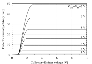
The insulated gate bipolar transistor or IGBT is a three-terminal power semiconductor device, noted for high efficiency and fast switching. It switches electric power in many modern appliances: electric cars, variable speed refrigerators, air-conditioners, and even stereo systems with switching amplifiers. Since it is designed to rapidly turn on and off, amplifiers that use it often synthesize complex waveforms with pulse width modulation and low-pass filters.
The IGBT combines the simple gate-drive characteristics of the MOSFETs with the high-current and low–saturation-voltage capability of bipolar transistors by combining an isolated gate FET for the control input, and a bipolar power transistor as a switch, in a single device. The IGBT is used in medium- to high-power applications such as switched-mode power supply, traction motor control and induction heating. Large IGBT modules typically consist of many devices in parallel and can have very high current handling capabilities in the order of hundreds of amperes with blocking voltages of 6000 V.
The IGBT is a fairly recent invention. The first-generation devices of the 1980s and early 1990s were relatively slow in switching, and prone to failure through such modes as latchup and secondary breakdown. Second-generation devices were much improved, and the current third-generation ones are even better, with speed rivaling MOSFETs, and excellent ruggedness and tolerance of overloads.[1]
The extremely high pulse ratings of second- and third-generation devices also make them useful for generating large power pulses in areas like particle and plasma physics, where they are starting to supersede older devices like thyratrons and triggered spark gaps.
Their high pulse ratings, and low prices on the surplus market, also make them attractive to the high-voltage hobbyist for controlling large amounts of power to drive devices such as solid-state Tesla coils and coilguns.
Availability of affordable, reliable IGBTs is a key enabler for electric vehicles and hybrid cars. Toyota's second generation hybrid Prius has a 50 kW IGBT inverter controlling two AC motor/generators connected to the DC battery pack.[2]
Contents |
History
The IGBT is a semiconductor device with four alternating layers (P-N-P-N) that are controlled by a metal-oxide-semiconductor (MOS) gate structure without regenerative action. This mode of operation was first proposed by Yamagami in his Japanese patent S47-21739, which was filed in 1968.[3] This mode of operation was first experimentally discovered by B. J. Baliga in vertical device structures with a V-groove gate region and reported in the literature in 1979.[4] The device structure was referred to as a ‘V-groove MOSFET device with the drain region replaced by a p-type Anode Region’ in this paper and subsequently as the insulated gate rectifier (IGR),[5] the insulated-gate transistor (IGT),[6] the conductivity-modulated field-effect transistor (COMFET)[7] and "bipolar-mode MOSFET".[8]
Plummer found the same IGBT mode of operation in the four layer device (SCR) and he first filed a patent application for the device structure in 1978. USP No.4199774 was issued in 1980 and B1 Re33209[9] was reissued in 1995 for the IGBT mode operation in the four layer device (SCR).
Hans W. Becke and Carl F. Wheatley invented a similar device for which they filed a patent application in 1980, and which they referred to as "power MOSFET with an anode region".[10] This patent has been called "the seminal patent of the Insulated Gate Bipolar Transistor."[11] The patent claimed "no thyristor action occurs under any device operating conditions." This substantially means the non-latch-up IGBT operation for the entire device operation range.
Devices capable of operating over an extended current range for use in applications were first reported by Baliga et al. in 1982.[5] A similar paper was also submitted by J.P. Russel et al. to IEEE Electron Device Letter in 1982.[12] The applications for the device were initially regarded by the power electronics community to be severely restricted by its slow switching speed and latch-up of the parasitic thyristor structure inherent within the device. However, it was demonstrated by Baliga and also by A.M. Goodman et al. in 1983 that the switching speed could be adjusted over a broad range by using electron irradiation.[6][13] This was followed by demonstration of operation of the device at elevated temperatures by Baliga in 1985.[14] Successful efforts to suppress the latch-up of the parasitic thyristor and the scaling of the voltage rating of the devices at GE allowed the introduction of commercial devices in 1983,[15] which could be utilized for a wide variety of applications.
Complete suppression of the parasitic thyristor action and the resultant non-latch-up IGBT operation for the entire device operation range was achieved by A. Nakagawa et al. in 1984.[16] The non-latch-up design concept was filed for US patents.[17] To test the lack of latchup, the prototype 1200V IGBTs were directly connected without any loads across a 600V constant voltage source and were switched on for 25 microseconds. The entire 600V was dropped across the device and a large short circuit current flowed. The devices successfully withstood this severe condition. This was the first demonstration of so-called "short-circuit-withstanding-capability" in IGBTs. Non-latch-up IGBT operation was ensured, for the first time, for the entire device operation range.[18] In this sense, the non-latch-up IGBT proposed by Hans W. Becke and Carl F. Wheatley was realized by A. Nakagawa et al. in 1984. Products of non-latch-up IGBTs were first commercialized by Toshiba in 1985.
Once the non-latch-up capability was achieved in IGBTs, it was found that IGBTs exhibited very rugged and a very large safe operating area. It was demonstrated that the product of the operating current density and the collector voltage exceeded the theoretical limit of bipolar transistors, 2x10⁵W/cm2, and reached 5x10⁵W/cm2.[1][18]
Device structure
An IGBT cell is constructed similarly to a n-channel vertical construction power MOSFET except the n+ drain is replaced with a p+ collector layer, thus forming a vertical PNP bipolar junction transistor.

This additional p+ region creates a cascade connection of a PNP bipolar junction transistor with the surface n-channel MOSFET. This connection results in a significantly lower forward voltage drop compared to a conventional MOSFET in higher blocking voltage rated devices. As the blocking voltage rating of both MOSFET and IGBT devices increases, the depth of the n- drift region must increase and the doping must decrease, resulting in roughly square relationship increase in forward conduction loss compared to blocking voltage capability of the device. By injecting minority carriers (holes) from the collector p+ region into the n- drift region during forward conduction, the resistance of the n- drift region is considerably reduced. However, this resultant reduction in on-state forward voltage comes with several penalties:
- The additional PN junction blocks reverse current flow. This means that unlike a MOSFET, IGBTs cannot conduct in the reverse direction. In bridge circuits where reverse current flow is needed an additional diode (called a freewheeling diode) is placed in parallel with the IGBT to conduct current in the opposite direction. The penalty isn't as severe as first assumed though, because at the higher voltages where IGBT usage dominates, discrete diodes are of significantly higher performance than the body diode of a MOSFET.
- The reverse bias rating of the N- drift region to collector P+ diode is usually only of 10's of volts, so if the circuit application applies a reverse voltage to the IGBT, an additional series diode must be used.
- The minority carriers injected into the n- drift region take time to enter and exit or recombine at turn on and turn off. This results in longer switching time and hence higher switching loss compared to a power MOSFET.
- The additional PN junction adds a diode-like voltage drop to the device. At lower blocking voltage ratings, this additional drop means that an IGBT would have a higher on-state voltage drop. As the voltage rating of the device increases, the advantage of the reduced N- drift region resistance overcomes the penalty of this diode drop and the overall on-state voltage drop is lower (the crossover is around 400 V blocking rating). Thus IGBTs are rarely used where the blocking voltage requirement is below 600 V.
IGBT models
Rather than using a device physics-based model, SPICE simulates IGBTs using Macromodels, a method that combines an ensemble of components such as FETs and BJTs in a Darlington configuration. An alternative physics-based model is the Hefner model, introduced by Allen Hefner of the NIST. It is a fairly complex model that has shown very good results. Hefner's model is described in a 1988 paper and was later extended to a thermo-electrical model and a version using SABER.[19]
Usage

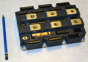
IGBT-Module (IGBTs and free wheeling diodes) with a rated current of 1200 A and a maximum voltage of 3300 V
|
Opened IGBT module with four IGBTs (half H-bridge) each rated for 400 A 600 V
|
See also
- Bipolar junction transistor
- Bootstrapping
- FGMOS
- Power electronics
- Power MOSFET
References
- ↑ 1.0 1.1 A.Nakagawa et al., "Safe operating area for 1200-V non-latch-up bipolar-mode MOSFETs", IEEE Trans. on Electron Devices, ED-34, pp.351-355(1987)
- ↑ Wikibooks, Toyota Prius, How it works
- ↑ Yamagami's patent can be searched by inputting "Kind code" B, "Number" S47-21739 in the data base
- ↑ B. J. Baliga, “Enhancement and Depletion Mode Vertical Channel MOS Gated Thyristors”, Electronics Letters, Vol. 15, pp. 645-647, September 27, 1979.
- ↑ 5.0 5.1 B. J. Baliga, et al., “The Insulated Gate Rectifier”, IEEE International Electron Devices Meeting, Abstract 10.6, pp. 264-267, 1982.
- ↑ 6.0 6.1 B. J. Baliga, “Fast Switching Insulated Gate Transistors”, IEEE Electron Device Letters, Vol. EDL-4, pp. 452-454, 1983.
- ↑ J. P. Russell, et al., “The COMFET: A New High Conductance MOS Gated Device”, IEEE Electron Device Letters, Vol. EDL-4, pp. 63-65, 1983.
- ↑ A.Nakagawa et al., High voltage bipolar-mode MOSFETs with high current capability", Ext. Abst. of SSDM, pp.309-312(1984)
- ↑ B1 Re33209 is attached in the pdf file of Re 33209
- ↑ U. S. Patent No. 4,364,073, Power MOSFET with an Anode Region, issued December 14, 1982 to Hans W. Becke and Carl F. Wheatley
- ↑ "C. Frank Wheatley, Jr., BSEE". Innovation Hall of Fame at A. James Clark School of Engineering. http://www.eng.umd.edu/ihof/wheatley.htm.
- ↑ J.P. Russel et al., "The COMFETs - a new high-conductance MOS-gate device," IEEE Electron Device Lett., vol. EDL-4, pp.63-65, 1983
- ↑ A. M. Goodman et al., "Improved COMFETs with fast switching speed and high current capability," IEEE International Electron Devices Meeting Technical Digest, pp.79-82,1983
- ↑ B. J. Baliga, “Temperature Behavior of Insulated Gate Transistor Characteristics”, Solid State Electronics, Vol. 28, pp. 289-297, 1985.
- ↑ Product of the Year Award: “Insulated Gate Transistor” General Electric Company, Electronics Products, 1983.
- ↑ A. Nakagawa et al., "Non-latch-up 1200V 75A bipolar-mode MOSFET with large ASO", IEEE International Electron Devices Meeting Technical Digest, pp.860-861,1984.
- ↑ A.Nakagawa, H. Ohashi, Y. Yamaguchi, K. Watanabe and T. Thukakoshi, “CONDUCTIVITY MODULATED MOSFET” US Patent No.6025622(Feb.15, 2000), No.5086323 (Feb.4, 1992) and No.4672407(Jun.9, 1987)
- ↑ 18.0 18.1 A. Nakagawa et al., "Experimental and numerical study of non-latch-up bipolar-mode MOSFET characteristics" IEEE International Electron Devices Meeting Technical Digest, pp.150-153, 1985
- ↑ A. R. Hefner, Jr., et al., “An Experimentally Verified IGBT Model Implemented in the Saber Circuit Simulator”, IEEE Transactions on Power Electronics, Vol 9, No 5, pp. 532-542, 1994.
Literature
- Dr. Ulrich Nicolai, Dr. Tobias Reimann, Prof. Jürgen Petzoldt, Josef Lutz: Application Manual IGBT and MOSFET Power Modules, 1. Edition, ISLE Verlag, 1998, ISBN 3-932633-24-5 PDF-Version
External links
- About the inventors
- Device physics information from the University of Glasgow
- Spice model for IGBT
- Insulated Gate Bipolar Transistor (IGBT) Basic Ixys Corporation Application note IXAN0063
- Cooling IGBT Modules
- Using IGBT Modules - Powerex
- IGBT and control input circuit for PWM applications